One for all: What the SAF production line consists of and what it can do
At Start A Factory we have the opportunity to manufacture your demonstrator on an industrial level on the production line. The line is the heart of our hall, which is why we will describe the functionality and the manufacturing process of a printed circuit board in more detail below. The process consists of three steps - starting with the paste application, followed by the assembly, and then the vapor phase.
The paste application
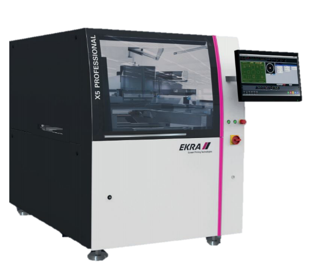
The first machine is an Ekra X5 Professional. This is a solder paste printer that is mainly used to apply solder paste to printed circuit boards.
For this, you need a suitable circuit board and a suitable stencil. With this stencil, a solder paste is applied to the circuit board. In principle, the paste is pressed through the stencil and then lands at the appropriate points on the circuit board. It is possible to print on many different materials - this can also be a soft material that is placed on a fixed carrier board for printing.
The solder paste used for this purpose is available in different variants. This depends on how the stencil is structured and how large the openings are. Above a certain size, a solder paste with a finer grain size must be used. This is why solder paste is also divided into T4, T5 and T6 - the higher the number, the finer the paste.
The machines are connected with so-called conveyors, which transport the printed circuit boards to the next machine. From the solder paste printer, the boards are then transported to the automatic placement machine from Fuji.
The placement
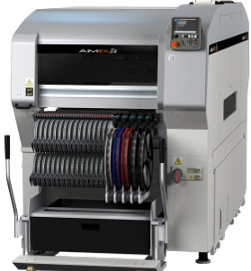
This is an IMAX 2S. Basically, the components are inserted into the machine in so-called reals, which are basically rolls on rolls that look like film reels.
These are then inserted or threaded into feeders accordingly. From these feeders, the machine can pick up the components with its head or with the individual nossels by sucking them in with a vacuum, and then transport them over the camera. In the process, the camera looks at the component from below and checks whether it is the right one and whether the alignment is correct.
If everything is correct, then the component can be placed in the correspondingly programmed positions on the PCB. For the various large components, there are also correspondingly different sized nossels to be able to pick up the components more easily.
Ideally, solder paste from the previous device has already been applied to the PCB. On the screen you can see what the machine is doing, what error messages are present and what the camera of the machine sees. Only one plate is loaded at a time. The maximum speed is 17,500 parts per hour. The cost of programming and setting up the machine is usually much higher than the resulting placement time. The placement is usually done in a few (1-3min) minutes. Programming is more time consuming and can take one to two days.
The printed circuit board has been printed in the printer up to now, and the components have been placed by the automatic placement machine. The next step is the melting of the solder paste. For this, the board goes into the appropriate oven. In this case it is a vapor phase oven from the company IBL - BLC 620I.
The vapor phase
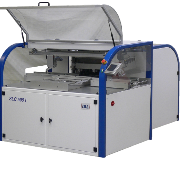
This vapor phase contains a vapor phase liquid that boils at 240°C and then generates corresponding vapor in the furnace chamber. The board is moved into the chamber, and the surrounding vapor transfers its heat and energy to the board and the components. During the process, the solder paste heats up and then melts accordingly.
Since the PCB is metallized and the solder paste and the components have connection pads that are also metallized, the solder paste melts between them and only wets the pads or the contact surfaces of the components. This prevents the solder paste from spreading over the rest of the PCB. In addition, a solder-stop lacquer is applied to the PCB, which also prevents the solder paste from moving somewhere other than where it is supposed to go. After the process, the PCB is still very hot. To cool it down, there is a so-called intermediate chamber. Depending on the size and the thermal capacity, you should wait a while before you can take the board into your own hands.
The advantage of the vapor phase is that the vapor can never get hotter than this 240°C, since it is not physically possible. This means that no overheating can take place, since the heating of the components or the PCB and the solder paste also only takes place at most within this range. Another advantage is the size. The steam chamber itself has only a small size - (the footprint is 1.50m*1.50m). In addition, the steam phase is relatively quiet, since only the steam is brought to a boil.
The whole line, which has just been presented, is the standard or minimum configuration. Of course, the whole setup could be extended with various devices, such as control devices or measuring devices between the individual stations, measuring devices at the end of the line, X-ray, automatic optical inspection, or test systems that check the function of the board at the end.
There are countless possibilities to extend the line. But basically, the three devices are sufficient for the time being to produce a functioning circuit board. Curious now? Then get in touch and maybe we can realize your hardware idea together!